Monday, 17 December 2012

MIPS


Hello guys. We meet again, now discussing over the most important topic in Computer Organization and Architecture subject. It is no other but the MIPS. MIPS are the abbreviation of Microprocessor without Interlocked Pipeline Stages. Internally, it is a reduced instruction set computer (RISC) instruction set architecture (ISA) developed by MIPS Technologies.
There are some basic implementations of MIPS instruction sets to be fully acknowledged.
1.    Memory reference : lw, sw
2.    Arithmetic / logical : add, sub, and, or, slt
3.   Control transfer : beq, j

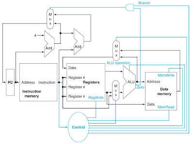
The instructions are executed for PC involving instruction memory and fetch instruction and for register numbers including register file and reading registers. The execution always depends on the instruction class itself. To calculate arithmetic result, memory address for load or store and branch target address, the ALU must be used. Then, after calculated the data memory will then be accessed for load or store.

Here I provide you an overview of a CPU:


Next is the figure of the multiplexers:


The data lines in the circuit cannot be wired together, as logic elements must be added. Those elements can be chosen from the multiple sources and steers one of those sources to its destination. The selection task is done by using multiplexor or can be called a data selector. Next figure is the basic implementation of the MIPS subset with multiplexers and control lines. There are three multiplexers altogether in the figure.


Now I’m going to give short explanations about the multiplexers’ functions embedded in the circuit.
1.                1st multiplexer (Mux) – controls what value replaces the PC
2.                Middle Mux – steer the output of ALU or the output of the data memory for writing into the register file.
3.                Bottom Mux – determine whether the 2nd ALU input is from the registers or from the offset field of the instruction.


Now, let’s move on to one other interesting subtopic in this topic. What do you know about R-Format instructions? It’s simple! These instruction formats reads two register operands for every single 5bits, but performs the arithmetic operation for every 6bits and then write the output of the operation in a form of 5bits register.
Below is the data-path of the R-Format instructions:


 The operation of this r-format instruction starts right when the instruction is fetched and the PC id done incremented. The, the two registers of the register file will be read before setting the RegDst, RegWrite and ALUOp. After that, the data read will be operated by the ALU by using the function code in order to get the ALU function be generated. Finally, the result from ALU will be written down in the register file to select the destination register.

Next, let us discuss about the load or store instructions in MIPS. For load instruction, register operands will be read before calculating the address using 16-bit offset. It also uses ALU but the sign-extend one. The, it will read the memory before finally updating the register. It is slightly different for store function. Firstly, it read the register operands before also calculating the address, also using sign-extend 16-bit ALU offset. But there’s a ‘but’! The store function will then write the register value to memory. Below is the load/store data-path:


Other than those instruction operations, there is also branch instruction for you to pay more attention. In branch, the register operands will firstly be read, and then be compared amongst them by using ALU to subtract and checking the Zero output of the operation. Finally, the target address will be calculated for sign-extend displacement. For a word displacement, the address calculated need to be shifted by two places. Then, the address will be added to PC+4 after being calculated by instruction fetch. As simple as that!
Below is the example of Branch-on-Equal (beq $t1, $t2, offset):


Last but not least is the jumps implementation. Take note that jump uses word address. It updates PC with combination of ‘top 4 bits of old PC’, ‘a 26-bits jump address’ and ‘00’. Jumps need an extra decoded control signal from opcode to be operating. Here is a load/store data-path added with Jumps.


Sunday, 16 December 2012

Input/Output Architecture


Hello! Meet us again, discussing about another topic of Computer Organization and Architecture called Input / Output Architecture. What is input? And what is output? For sure, everybody know input devices right? It includes keyboard, mouse, scanner, CD-Rom and also Game Controller. They are the devices the user used to enter instructions to machine. In the other hand, output devices such as monitor, printer, disk drive, floppy drive, CDRW-Rom and speakers are used to produce the data from a machine.

Input/Output devices can be characterized into behavior, partner and data rate. Behavior includes input, output and storage. Partner is either the human or the machine, whereas data rate is measured whether in bytes/sec or transfer/sec. The Input / Output bus connection is figured out as below:


There are 5 main functions of I/O modules that are control and timing, CPU communicating, device communicating, data buffering and error detection.

In ‘control and timing’, CPU asks the module of I/O to check the status of attached device. After the modules reports the ready status, CPU will request for data transfer to module. The I/O modules will then gather the data before transferring it to the CPU.

In ‘CPU communication’, there are four tasks which are Command Decoding, Device Communication, Data Buffering and Error Detection. In command decoding, the reading or writing of data exchange will take place. During this process, if the peripherals are slow, status reporting will be executed. Address recognition also take place in the mean time. Next, device communication usually includes command, status information and data transfer. Data buffering is one needed to solve speed problem. Lastly is the error detection such as paper jam and bad data.

This is the structure of Input / Output Module:


The characteristic of I/O System is essential to be followed. The first one is dependability, which is very important for storage devices. Next one is the performance measures.

There are two types of bus including Processor-Memory Buses and I/O Buses. Processor-memory bus is short but has a high speed of data exchange, since its design matches the memory organization. I/O bus is longer, allowing multiple connections and is specified by standard for interoperability. This bus connect to processor-memory bus through a bridge.

There are several things in bus signals and synchronization. The data lines carry address and data whether they are multiplexed or separated. The control lines indicate the data type and also synchronize transactions. There are two type of synchronization that is synchronous which uses a bus clock and asynchronous that uses request control lines for handshaking.

Other than that, I/O is mediated by the operating system. Five techniques of I/O are programmed I/O (polling) which check I/O status periodically, interrupt driven I/O, direct memory access which helps to free CPU from pure data transfer tasks, memory mapped I/O in which address translation mechanism is used by the OS to make register only accessible to kernel and also the isolated I/O which separates the instructions to access I/O registers in kernel mode.

There are two I/O transfer mode named as serial and parallel transfer. In serial transfer, asynchronous clocking master clock the transfer and then slave derive clock from the master, while the synchronous clocking is independent that makes verification by synchronization pattern. In the other hand, data transfer in parallel transfer involves sector reading and sector writing. The controlling includes disk seek and then the transfer integrity transfer parity and also encodes the data.

I/O performance depends on the hardware, software and workload that request rates and patterns of the computer itself. I/O throughput is measured with constrained response-time.

Amdahl’s Law states that I/O performance can’t be neglected because parallelism increases computer performance.

Next, I/O system design must be satisfying latency requirements for time-critical operations, maximization of throughput by balancing the remaining components in the system and sufficient analysis according to system loading.

Those are everything to be said about input / output architecture. Now you see, it's not that hard to be mastered as long as you really want it. That's all for now. 'Till later!
^_^ 

Language of the Computers


Hello. Here we go again. This time we’re going to discuss about no other but the language of the computer. Everybody does know that computers do not understand the daily English language human use. The users communicate with the computers by using specific machine language. Nah, now that’s the exact topic that we’re going to be discussing about here.

Now we’re introducing the Instruction Set Architecture or globally known as ISA. This ISA thing is seldom officially defining a ‘family’ of microprocessors that builds up a set of instruction to be used to communicate to a machine. The examples of ISA that are widely used are Intel x86 (IA32), Sun Spare, DEC Alpha, IBM/360, IBM PowerPC, M68K and DEC VAX. Formally and normally, the interface between a user and a microprocessor is defined by this instruction set. Internally, ISA includes instruction set, instruction encoding and some important rules of instruction using that are mnemonics, functionally and also the addressing modes.

Next is the introduction to the SPIM and MIPS. Generally, SPIM is the backward spelling of MIPS. SPIM is the simulator of MIPS that reads assembly language files of MIPS and then translates it to machine language. SPIM also executes the translated the machine language instructions before showing the contents of registers and memory. SPIM also works as the debugger that is able to support break-points and single-stepping. Other than that, SPIM provides basic operating system such as services and simple input/output. Besides, please be glad to use SPIM simulator because it is available for free online.

Right then after that, we’re discussing about the arithmetic operations in instruction language which includes addition, subtraction and many other. There will be three operands needed to operate the addition and subtraction where two operands acts as the sources whereas another one is the destination. For the code of [a,b,c], explaining a is the destination keeping the result of b plus c. As simple as that!

Now we move on to register operands. Arithmetic instructions of computer surely use register operands. For your information, MIPS has 32x32-bit of register files that are used for accessed data which numbered from 0 to 31. A 32-bit data is called a ‘word’. For temporary values, the assembler is named as $t0, $t1, $t2, $t3, $t4, $t5, $t6, $t7, $t8 or $t9. On the other hand, the assembler is named as $s0, $s1, $s2, $s3, $s4, $s5, $s6 or either $s7 if it’s a saved variable. Take note that the second Design Principle says that a smaller number produces a faster output. If a simple one states [add a,b,c ] like the previous example I gave explains ‘a’ stores the value of  ‘b’ + ‘c’, then [add $s0, $s1, $s2] means that $s0 takes the value of ‘$s1’ adds ‘$s2’.

To compare, registers are a lot faster than to be accessed than the memory. Os why use memory?

Next, let’s move on to the memory operands. Composite data like arrays, structures and dynamic data uses main memory. It is used for applying operations of arithmetic such as values loading from memory into registers and also result storing from register to the memory. In addition, memory is addressed in byte where each address identifies an 8-bit byte. Don’t forget that the addresses must be in a multiple of 4 single addresses to form a word aligned in memory.

The next one is about the representing instructions. Instructions are encoded in binary which is called as machine code or computer code. MIPS instructions are encoded as 32-bit instruction words. There are 3 instructions formats altogether, composing R-Format, I-Format and J-Format.

These are some simple formula and explanations over the all three instruction formats. The first one is the r-format instruction. Remember that when all operands in the MIPS code are registers, then the code must be not another but the r-format. The example of MIPS code using r-format instruction is as below.
Add $8, $9, $10

The second one is the j-format instruction. A code that uses this type of instruction format is the code that has one and only operand. For example is as below. As you see, the code contains one operand only.
J 10000

Last but not least is the i-format instruction. The rule of this type of format is the other than stated for r-format and j-format instructions.
bne $8, $9, -100
lw $8, 100 ($9)
addi $8, $9, 100

The next essential thing you need to know about language of the computers is addressing. The first type is the branch addressing where the instructions specify opcode, two registers and target address. Most of the branch targetsa re near the branch itself, either from the front or backward. If the branch target is too far ffset, the assembler will rewrite the code. For example,
beq $s0, $s1, L1     ->       bne $s0, $s1, L2
                        jL1

Next one is the jump addressing. Jump including ‘j’ and ‘jal’ targets can be anywhere to find in the text segment. To summarize, the addressing mode of computer instructions include all 5 mode altogether. There are register addressing, pseudodirect addressing, base addressing, immediate addressing and PC-relative addressing.

The code is said to be using register addressing mode when the code has the sources and destinations are all registers. The example is as follows.
add $8, $9, $10

Next, a machine code having one and only operand will be directly categorized as the pseudodirect addressing mode. Example:
j 10000

After that, let’s move on to the base addressing mode. A code using base addressing mode has its final operand having brackets on it. Example:
lw $8, 100 ($9)

The fourth one is the immediate addressing mode. If the final operand in the code is a constant, then the code is using this kind of addressing mode. Example:
addi $8,$9, 100

Finally, let’s talk about PC-relative addressing mode. The code’s output is a branch. For this mode, the code usually includes the operation of Branch on Equal (beq), Branch on Not Equal (bne) and so on that has the initial b. The example is as follow:
bne $8, $9, -100

In conclusion, we have three instruction formats and five addressing modes to be understood of. They are all as simple as a b c. You just need to put your interest and confide in yourself to improve. Okay, see you later in the next entry!
^_^ 

Monday, 3 December 2012

video assignment

Finally we made it this far! All praises to the Almighty. We were discussing on a topic in Chapter 4 and Chapter 5 as well involving MIPS in CoA subject.


Sunday, 21 October 2012

Arithmetic for Computers

Hello! We’re back again, now bringing up the second topic to be discussed about. We picked the second topic from our semester’s syllabus that is, Arithmetic for Computers (Number Systems and Operations)

From what we understand from the exact definition of arithmetic, it is actually the oldest and most elementary branch of mathematics that is used by almost every single studying person, for tasks ranging from simple day-to-day counting to advanced science and business calculations. It includes the study of quantity, especially as the result of operations that combine numbers. In common usage, it refers to the simpler properties when using the traditional operations of addition, subtraction, multiplication and division with smaller values of numbers.
So basically, arithmetic is all about numbers and operations involving numbers. As we always know, we humans use the decimal number system to perform arithmetic operations including every numbers to infinity. On the other hand, not for the computers, that uses the binary system, containing only two digits that are 0 and 1. We need a way to convert numbers from one system to another in order to allow computers to understand us.
All the number systems we use practically operate on some basic principles where each of it has a base as we will look at decimal with base 10, binary with base 2 and hexadecimal  owning base 16. The base denotes the number of digits and the powers to be used. Base 10 has 10 digits that are numbered from 0-9 and uses the powers of 10. However, base 2 has 2 digits that numbered from 0-1 and uses powers of 2 whereas base 16 has 16 digits which numbered from 0-F (where the letters A-F serve as the digits following 9), and uses the powers of 16.
Other than that, each of these systems of number is a positional notation system meaning that the location of a digit in the number determines its value. As an example, the value of 6 in the decimal number 631 is not the same as the value of 6 in 361 or 136.

So in this explanation part, we'll be using the decimal number system to show how the positional notation system works. Assuming that we have the number 631, what this number means? Each digit represents that digit itself amplifying the power of 10 represented by its position. Don’t forget that the decimal point is supposed to be on the right of the number if it is not explicitly shown. Starting at the decimal point and moving to the left, the columns represent increasing powers of 10. Now we are showing the steps.

102       101       100
6          3          1

The base of the numbers is 10 because the number is initially in decimal form, and the exponent (the superscript) tells what power of 10. The exponents increase by 1 with every move to the next position to the left. Note that the exponents also decrease by 1 with each column move to the right, so the first position to the right of the decimal place tells how many 10-1's are in the number, and the second position to the right of the decimal place tells how many 10-2's are in the number and so forth for other bases.
Recall that any number to the zeroth power is 1, and any number to the first power is that number itself. So the column labeled 100 denotes how many 1's are in the number, the column labeled 101 represents how many 10's are in the number, and the column labeled 102 shows how many 100's are in the number as shown below;
100's column              10's column                1's column
6                      3                                  1
Thus this number has 1 ones, 3 tens, and 6 hundreds, where
1 x 100 = 1 x 1 = 1
3 x 101 = 3 x 10 = 30
6 x 102 = 6 x 100 = 600
So by summing up all those numbers, we will get the number in base 10.
1 + 30 + 600 = 63110
But we basically do not put the subscript for base 10 because base 10 numbers are the numbers we are always using. On the other hand, we do for the other bases like 100011002, 112358 and AE4316. This is due to the using of these bases that is not too wide excluding for those who are involved with computers.


Operations on Integers
There are some operations in dealing with integers in number system. I’m sure every single studying person learn basic operation involving numbers, right. What else could it be other than addition, subtraction, multiplication, division and in this case we also had to deal with overflow in those operations.
Let’s get started with the simplest operation that is addition. If the yield is out of the range, there will be an overflow. Simply, adding positive and negative operands will result in no overflow. But adding two positive operands will result an overflow, but if only the yield sign is equal to 1. In the other hand, the operation of summing up two negative operands will result an overflow only if the result sign is 0.
Saem goes for subtraction operation of integers. There will be an overflow when the value produced is out of the range. There will be no overflow when the operation involves subtraction of two positive or two negative operands. But if the result sign is 0 after subtracting positive from negative operand, there will be an overflow. The overflow will also exist when the result sign is 1 after subtracting negative from positive operand.

Dealing with Overflow
Here are some ways to handle the overflow cases. Somehow, some languages such as C. will just practically ignore overflow. We can use MIPS addu, addui, subu instructions to deal with it. We can also use other languages as Ada and Fortran. But using these languages require a raising an exception. So it is quite difficult to be settled. We might also use MIPS add, addi, sub instructions for other incentive. Plus, we can invoke exception handler on overflow as one of the ways to deal with it. Next step is just by saving the PC in exception program counter (EPC) register.
As multimedia-majoring students, we absolutely need to know these, that arithmetic is such a basic thing in multimedia. It is the foundation that makes the media up, compiling those media becoming multimedia, such a perfect, attentive presentation medium to be used by us, the users. In this prospect, graphics and media processing operates on vectors of 8-bit and 16-bit data.
Next, let’s move on to multiplication operation of integers. As an example taken from our notes,

The upper operand is called multiplicand while the lower one is known as the multiplier. The length of product is the sum of operand lengths.

The next one is division operation. Note that if the divisor is less than or equal to its dividend bits, it will be 1 bit in quotient, and then subtracting the two operands. Otherwise, the other 0 bit in quotient, we will just bring them down next to dividend bit.


Floating Point

Floating points is the way of representation for non-integral numbers including smallest and largest numbers. As if in scientific notation;
–2.34 × 1056
+0.002 × 10⁻⁴
+987.02 × 10⁹

Floating point standard is defined by “IEEE Std 754-1985”. It is developed in response to divergence of representations which is a portability issues for scientific code. IEEE Std 754-1985 is now almost universally adopted. Other than that, there are two ways of representations the floating point standards those are single precision (32-bit) and double precision (64-bit).

Okay! Now we are finished with our short brief explanation about arithmetic involved in computers. We do hope that you understand and the information we have prepared will be able to help you in improving your understanding towards arithmetic Number System. A lot of thanks for spending your precious time to visit our page!
^_^


Monday, 8 October 2012

What is digital logic.

Most of us do not have the basic knowledge in Computer Organization and Architecture.
Hence, in this post, we are going to explain about one of the basic things on how the computer would operate. It is DIGITAL LOGIC.

So, basically, what is Digital Logic?

The theory is " Logic gates (or simply gates) are the fundamental building blocks of digital circuitry. As their name implies, they function by “opening” or “closing” to admit or reject the flow of digital information by using digital electronics, which are ; Gates, Decoders, Multiplexers."

But to make you understand better, ill explain these, a bit more detailed.

Digital logic is the basis for digital computing.It is basic the basic to understanding how circuit and hardware are connected to computer. The signals of digital logic is represented by using numbers which are zeros and ones (0s and 1s).

There are four type of gates; AND, OR, NAND, or NOT gate. These gates are to process signals which represent true or false by using Truth Table. Another ways to process the signal is by using the Boolean Algebra.


/WhatIs/images/and.gif (220 bytes)
AND gate

/WhatIs/images/or.gif (224 bytes)
OR gate

/WhatIs/images/not.gif (240 bytes)
NOT gate

/WhatIs/images/nand.gif (240 bytes)
NAND gate

/WhatIs/images/nor.gif (237 bytes)
NOR gate


TRUTH TABLE

Truth Table provide a method of accessing the validity or invalidity of performing any of the tasks to user requested. Each gates have two or more inputs excepts for NOT because it has only one input. Usually, the inputs are represented by using the letters A, B , and C. While the output is represented by using of any other letters. A Truth Table is the exact way to show the function of the logic gates. It shows the input and the output states for every possible combination. The symbol 0 represents FALSE and 1 represent TRUE.


BOOLEAN 

Boolean Algebra or Boolean Logic resembles the ON and OFF circuit which all the signals are classified as either

 Law:

Identity law: A + 0 = A and A & 1 = A.

Zero and One laws: A + 1 = 1 and A & 0 = 0.
Inverse laws: A + A’ = 1 and A & A’ = 1.
Commutative laws: A + B = B + A and A & B = B & A.

Associative laws: A + (B + C) = (A + B) + C and A & (B & C) = (A & B) & C.

Distributive laws: A & (B + C) = (A & B) + (A & C
and
A + (B & C) = (A + B) & (A + C).

DECODER

A decoder is a circuit that converts code to signals (0s or 1s). For example, a decoder can convert the n-bit input into a binary signal. There are types of decoder, but most of decoders give only one n-input and 2,4,6, ... outputs.

This is the example :


 So, are you clear now? But wait up, we're not done yet. So lets continue to the last digital electronic which is ;


MULTIPLEXER


A multiplexer (MUX)  is a device that select several analog or digital input signals and translate the inputs that has been determined as the output into a single line. So basically, an MUX consusts of 3 parts;
1. A decoder that generates n-signals, which each of it indicates a different input value.
2. An array of AND gates, which each ot it combines one of the inputs with a signal from the decoder.
3. A single LARGE OR gate that incorporates the outputs, of the AND gates.


Anddd, we are done! I hope that you have already understood what"Digital Logic" actually is. For more info about the architecture and organization of computer, stay tuned! We have lots to share! Toodles!


Nur Ezany bt Elias
B031210213
BITM S1G2


Sunday, 30 September 2012

Saying hello!

It's officially for BITS 1213 - Computer Organization and Architecture assignment.
What about our group? We have 4 of us…
1.   Nurul Annisa Alia binti Roslan, born on 3rd of July 1993.
2.   Nur Ezany bnti Elias, born on July 19th of 1993.
3.   Fatin Najwa Binti Sukaimi, born on 5th of September 1993.
4.   Nur Iylia Binti Zubir, born on September 21st of 1993.

making all of us of the same age. We’re from BITM Section 1 Group 2 (S1G2).